Waveguide-integrated Ge p-i-n photodetectors on a Si platform
Donghwan Ahn, Jifeng Liu, Ching-yin Hong, Mark Beals, Jurgen Michel, Lionel C. Kimerling
Sponsor: DARPA—EPIC program
For an electronic-photonic integrated circuit on-chip, an essential component is the waveguide-integrated photodetector on a Si CMOS platform to convert optical signals to electrical ones. Ge photodetectors epitaxially grown on a Si substrate have demonstrated promising performances in our previous research work. Now we are developing and demonstrating Ge photodetectors integrated with high index contrast waveguides on a Si platform.
Figure 1 shows two waveguide-detector coupling schemes that we have developed: (1) evanescent coupling, where the light couples evanescently from the waveguide to the detector; and (2) butt-coupling, where the output end of the Si waveguide directly inputs to the Ge photodetector. In the evanescent coupling scheme, we have demonstrated waveguides placed on top or at the bottom of the Ge photodetectors, shown in Fig. 1a and 1b, respectively. We have achieved a responsivity of >1.0 A/W at wavelengths of approximately 1550 nm and a bandwidth on the order of several GHz with both evanescent coupling and butt-coupling schemes. The coupling efficiency between the waveguide and the detector is greater than 90%.
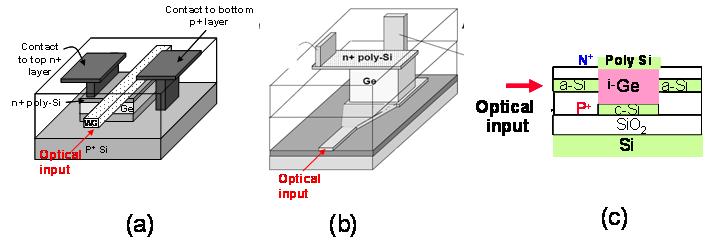
Figure 1: Schematic diagrams showing different waveguide-detector coupling schemes: (a) evanescent coupling, waveguide on top of the Ge detector; (b) evanescent coupling, waveguide at the bottom of the Ge detector; and (c) butt-coupling scheme, output end of the waveguide directly inputs to the detector.
Figure 2 shows an example of the performance of an evanescently coupled photodetector, where a SiON waveguide is placed on top of the Ge photodetector. The responsivity is >1.0 A/W in a broad wavelength range of 1480-1570 nm, and does not show the roll-off at ~1540 nm that is typical for normally incident Ge-on-Si photodetectors. This is because the optical path length in waveguide-integrated Ge photodetectors is determined by the length of the Ge photodetectors (>5 microns), which is much larger than the case of vertical incidence where the optical path length is determined by the thickness of the Ge film (~1 micron). On the other hand, the carrier collection direction is perpendicular to the wafer surface and the transit time remains short since the thickness of the Ge film is only 1 micron. As shown in Fig. 2b, the bandwidth is ~7 GHz even at 0V bias. Therefore, waveguide-integrated Ge photodetectors demonstrate high efficiency, high speed and low operation voltage at the same time. These features are excellent for on-chip applications. Currently, the speed of these devices are limited by the relatively large contact pads. When fully integrated with other electronic components these pads are no longer necessary and the bandwidth of the device can be greatly improved.
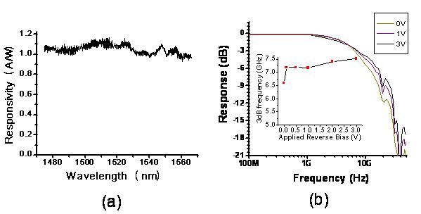
Fig. 2. (a) Responsivity vs. Wavelength, and (b) bandwidth vs. reverse bias of a Ge p-i-n photodetector integrated with a SiON waveguide on a Si platform.