Large Electro-optic Effect in Tensile Strained Ge-on-Si Films
S. Jongthammanurak, J. Liu, K. Wada, D.D. Cannon , D.T. Danielson, D. Pan, L.C. Kimerling, and J. Michel
Sponsor: DARPA-EPIC
Silicon-based integrated photonic circuits represent a promising technology for high capacity data communication and high speed parallel signal processing.[1] Optical modulators are a key component in these integrated circuits for encoding information on optical carriers. Existing silicon modulators use the plasma dispersion effect to modulate refractive index. The bandwidth limit of these devices (~1-10GHz[2, 3]) is determined by the slower rate of either the injected carrier sweep-out or electron-hole recombination process. While this device represents a new paradigm for electro-optic silicon-based components, its footprint and power dissipation do not scale to levels of high density integration. This report is the first of a study of electric field modulation of refractive index in silicon-based materials for high-speed applications. We find that germanium integrated monolithically on silicon exhibits a large, field-modulated electro-optic effect in the weakly absorbing regime.
The field dependence of absorption in the Ge films was measured from spectral responsivity measurements of Ge-on-Si p-i-n diodes. The experimental data were analyzed using the generalized Franz-Keldysh formalism and independently measured valence band edge shifts of the light- and heavy-hole energy positions in response to biaxial stress, using Photoreflectance technique. An electric field of 70 kV/cm increased the absorption coefficient from 62 cm-1 to 230 cm-1 at 1647 nm, in very good agreement with the theory (Fig. 1). At 1647 nm, the electro-optic coefficient Dn/F for the strained Ge film is 280 pm/V, as compared to 160 pm/V for unstrained Ge. The measured Da/a ratio for the strained and unstrained Ge films are 3.03 and 1.11, respectively (Fig. 2). These results show that the Ge-on-Si epitaxial films have significant potential for efficient CMOS -compatible, field-induced optical modulator devices.
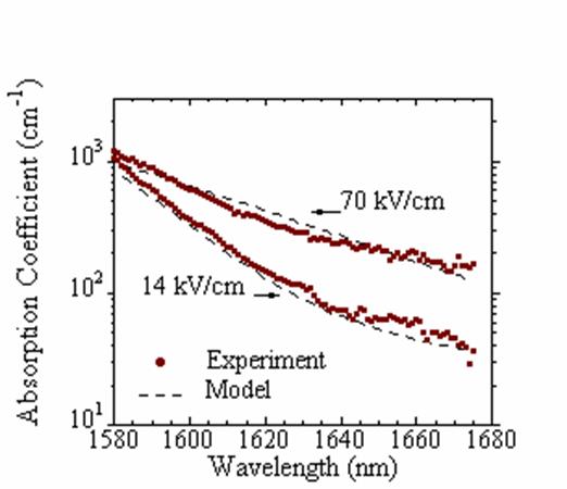
Fig. 1: Excellent fit of experimental data to the model based on the generalized Franz-Keldysh formalism without fitting parameters.
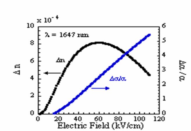
Fig. 2 Application of the model to predict D n and D a / a at 1647 nm wavelength as a function of the applied electric field.
References:
[1] R.A. Soref, Proceedings of the IEEE, 81, 12 (1993).
[2] A. Liu, R. Jones, L. Liao, D. Samara-Rubio, D. Rubin, O. Cohen, R. Nicolaescu and M. Paniccia, Nature , 427, 615-618 (2004).
[3] Q. Xu, B. Schmidt, S. Pradhan and M. Lipson, Nature, 435, 325-327 (2005).