Silicon Oxynitride Waveguide Materials for Microphotonics
J. Sandland, M. Stolfi, V. Nguyen, X. Duan, K. Lee, M. Nava Marenzi, A. M. Agarwal, K. Wada, J. Michel and L. C. Kimerling
Sponsors: Draper Laboratory, MARCO Focused Research Center Program—Interconnect, Pirelli Labs
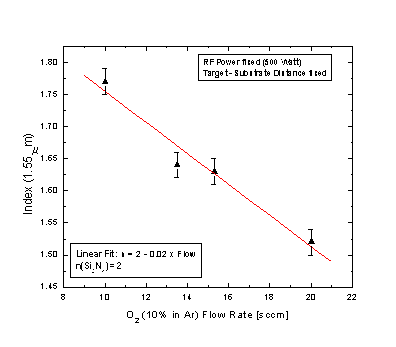
High performance waveguide materials must combine low optical loss with the flexibility to fabricate a wide variety of active and passive devices on a single materials platform. With a refractive index tunable between 1.46 and 2.3, silicon oxynitride provides this flexibility. However, current methods used to process silicon oxynitride introduce excessive amounts of hydrogen that increases the amount of transmission loss and forces the use of very high temperature anneals to reduce the hydrogen concentration and reduce the loss. Sputter deposition provides an alternative to these traditional deposition methods; it has the potential to produce high quality, low loss silicon oxynitride waveguides with virtually no hydrogen incorporation and easily controlled refractive indices. Preliminary studies have shown sputtered silicon oxynitride to be a good potential waveguide material. Low birefringence films have been produced over a wide range of refractive indices by reactive RF sputtering in an argon and oxygen ambient from a silicon nitride target. Figure 1 shows the measured refractive index of several silicon oxynitride films fabricated using a range of oxygen gas flow rates. The linear decrease of the refractive index with increasing oxygen gas flow rate demonstrates the ease in tuning the refractive index between the values for silicon nitride and silicon dioxide. Future studies will focus on producing waveguides using these sputtered oxynitrides as core materials.