Photonic Crystal and Microcavity Devices
Y. Yi, L. Dal Negro, K. Chen, M. Lipson, S. Akiyama, X. Duan and L. C. Kimerling
Sponsor: NSF, MRSEC
A photonic crystal is a periodic composite of high and low refractive index (dielectric) materials that, as a medium, influences the propagation of light, in a manner analogous to the influence of solid state periodic potentials on electron propagation. Analogous to the formation of semiconductor electronic (1) conduction band, (2) valence band and (3) bandgap, a photonic crystal can be designed to have a (1) high dielectric band, (2) low dielectric band, and (3) photonic bandgap (see Fig.1).
Historically the 1D version of a photonic crystal has been better known as the Bragg reflector or mirror, a periodic structure composed of two alternating layers of thickness t=λ/4n, where n is the refractive index of the layer and λ is the free space wavelength for which optimal reflection has been designed.
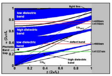
Fig. 1(a) The Photonic Band Diagram, plotting the (angular) frequency \omega versus propagation constant beta of allowed states (blue shade). Inhibited, or bandgap states, are shaded white. The black color line within the bandgap is the dispersion relation of defect-band states.
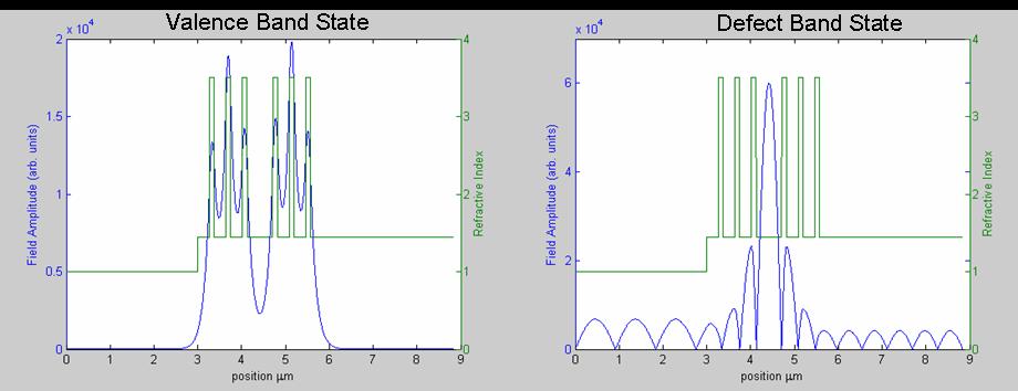
Fig. 1(b) Schematic depiction of the (electric) field distribution of a characteristic valence band state and defect band state within a photonic crystal containing a non-periodic defect.
Photonic crystals signal a new design paradigm for Microphotonics that enables unprecedented micron-scale light manipulation, by means of sub-micron scale materials processing. Key applications of this novel technology include:
- microcavity structures for low threshold light sources,
- photonic crystal waveguides for low dielectric core or hollow-core bio-sensing applications,
- WDM multichannel tunable filters, and
- complex (i.e. quasi-periodic) photonic structures for cavity-less active or multi-resonant devices.
Microcavity Devices
Microcavity Devices are 1D photonic crystals structures with a defect layer, whose transmission properties are characterized orthogonal to the defect layer (and Bragg mirror layers).
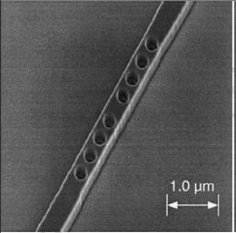
Fig. 2(a) Plane-view SEM image of in-plane microcavity device etched within a Si waveguide.
![]()
Fig. 2(b) Transmission spectral profile through this waveguide structure.[1]
The microcavity devices in Figs. 2 and 3 demonstrate microcavity transmission properties in structures designed to be in-plance (Fig. 2)[1] and out-of-plane (Fig. 3).[2] As the experimentally verified transmission spectra of Fig. 2(b) indicates, the transmission properties of these two structures are simply those of a Bragg reflector combined with a defect layer of thickness λ/2n, where λ is the free space wavelength that will be resonantly confined within the defect layer.
The Si waveguide microcavity structure of Fig. 2 represents a record low modal volume of 0.055 um3, with a resonant confinement Quality Factor of Q=265.
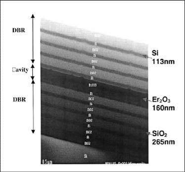
Fig. 3: Cross-section SEM image of out-of-plane microcavity device comprised of Si/SiO2 Bragg layers and an Er2O3 defect layer (structure grown by sputtering).
Potential applications for microcavity devices include WDM filter transmission and Vertical Cavity Surface Emitting Laser (VCSEL) light sources for a high bandwidth microphotonic/free space transceiver.
The Photonic Crystal Waveguide
A popular example of a photonic crystal device is the photonic crystal fiber, successfully demonstrated by Fink, Joannopoulos et al. at MIT. Fig. 4 shows the first demonstration of a photonic crystal waveguide, a planar-processed version of this device, developed by the EMAT group.[2]
Photonic crystal fibers and waveguides are 1D photonic crystal structures with a defect layer, whose transmission properties (propagation constant \beta) are characterized along the defect layer (and Bragg mirror layers).
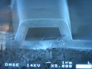
Fig. 4: An SEM picture of a Photonic Crystal channel waveguide depositied on a Si substrate. The photonic crystal waveguide cladding layers are Si and Si3N4; the waveguide core layer is SiO2.[2]
The photonic crystal waveguide in Fig. 4 is comprised of a conformal cladded 1D Si/Si3N4 photonic crystal; the waveguide core is a defect layer of SiO2.
To characterize the photonic crystal confinement mechanism for waveguide propagation, we measured the effective group index of the propagating mode in a 1D structure (by coupling in light by means of a prism coupler). The measured effective group index is less than that of either the Si or Si3N4 cladding layer refractive indices, unconditionally demonstrating the photonic band gap guiding principle: light can be confined and propagated within lower dielectric media. Propagation losses as low as 0.5 dB/cm have been achieved in asymmetric Photonic Crystal waveguides.
Potential applications for Photonic Crystal Waveguides include high power transmission, low dispersion elements, and high confinement nonlinear devices.