Waveguides and Integrated Photodetectors for On-chip Optical Clock Signal Distribution
Donghwan Ahn, Ching-yin Hong, Jurgen Michel, Lionel C. Kimerling
Electrical interconnects are the current platform for clock signal distribution across a chip, which governs the internal operations of a microprocessor in a synchronous chip design. However, the continuous enhancement of electrical clocking speed is expected to face limitations in the near future. Electrical clocking will have difficulties arising from jitter and skew of the signal and an increase in power consumption as the clocking frequency is increased.
A solution to overcome this barrier is optical clock signal distribution. Using photons instead of electrons can help reduce skew and jitter of clocking and enables the increase of the clock signal frequency well above 10 GHz while keeping the power consumption and heat generation low.
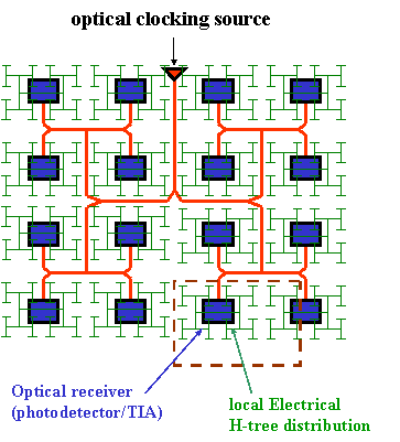
Figure 1: Schematic of optical clocking and H-tree waveguide structure.
As a signal-distributing component of optical clocking circuitry, we fabricated silicon CMOS-compatible SiO x N y H-tree optical waveguide networks and we observed successful transmission of light to all 64 fanouts. Uniform and low-loss signal distribution is required for the waveguide structure. By designing a novel extended offset splitter, we created a zero splitter angle and reduced the splitting loss to < 3% and furthermore, reduced the sensitivity of the power-splitting ratio to asymmetric patterning errors. Both simulation and experiment demonstrated that a power-split uniformity of 49:51 or better is achievable.
One of the important technological components in optical circuitry is the integration of photodetectors and waveguides. It also benefits detector performance by circumventing the usual trade-off between responsivity and bandwidth. Since it is important to achieve efficient and uniform optical coupling between waveguides and photodetectors, we are investigating the coupling behavior between SiON/Si 3 N 4 /Si waveguides and group IV absorbing materials such as Si/Ge photodiodes, which can be monolithically integrated with a Si CMOS chip. One example is evanescent wave coupling structures with SiON waveguide and Si vertical p-i-n photodetector has been fabricated, as schematically shown in Fig. 2(a). We have achieved over 90% coupling efficiency from waveguide to Si photodetector. Other novel coupling structures with Si waveguide and Ge photodetector are being processed with a target of high coupling efficiency and high-speed performance.
Theoretical studies based on analytic modeling and BPM/FDTD optical simulations have been done. As one example, Fig. 2(c) shows that the coupling between a SiON waveguide and a SOI detector has a discrete coupling behavior dictated by phase matching conditions.
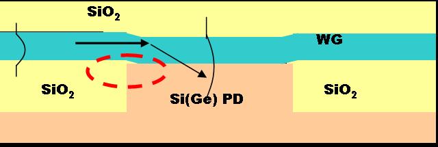
Fig. 2(a) Schematic of waveguide photodetector integration structure.
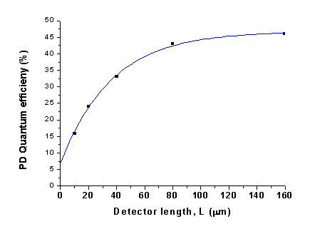
Fig. 2(b) Quantum efficiency vs. the coupling length of detector, which was coupled with 1.2 um x 1.2 um SiON (n = 1.52) waveguide.

Fig. 2(c) Calculated dependence of coupling efficiency on Si layer thickness in SOI waveguide photodetector.