Multispectral Infrared Detector Arrays (MIDAS)
Xiaochen Sun, Juejun Hu, Anuradha Agarwal, Rupa Das, Jeff Viens and Lionel C. Kimerling
Sponsor: Deshpande Center, Lincoln Laboratory
The objectives of the project are: 1) to further develop the intelligence applications of infrared focal plane arrays by developing and characterizing the multi-spectral responsivity of a AsSeTe:Cu photonic crystal pixel, mounted on a silicon chip; and 2) to explore the possibility of bringing the large-area multi-spectral infrared array technology from specialty to commodity pricing, and hence generate new opportunities in this high-growth market. The work explores the development of large-area monolithic photodetector arrays combining near-IR, mid-IR and far-IR detection. To address the problems of high cost and limited intelligence capabilities of current infrared technologies, our design explores a way to utilize the asset base of silicon technology to significantly reduce the cost, and improve performance characteristics, of large-area multi-spectral infrared focal plane arrays via the use of photonic crystal pixels made of amorphous semiconductors integrated on a silicon platform. This novel photoconductor pixel exploits resonant cavity enhancement (RCE) for multispectral capability, high quantum efficiency, and dramatically suppressed shot noise. As we know, in a quarter-wavelength stack (1-D photonic crystal), standing wave patterns (defect modes) form at resonant wavelengths when defect layers are present. By tuning the thicknesses and positions of photoconductive layers optimally with respect to the modal overlap with the defect modes, each photoconductive layer will selectively absorb only one specific resonant wavelength. Besides multispectral capability, the proposed design features enhanced optical absorption due to RCE effect and allows the use of thinner photoconductive layers which significantly reduces shot noise and improves the performance of photoconductive detectors.
Electrically-connected sensor pixel arrays incorporating SiO2 and Si3N4 periodic photonic crystals and two a-Si photoconductive layers were fabricated to demonstrate the mode discrimination concept (Fig. 1). The entire fabrication process was compatible with standard CMOS technologies, which projects significant cost reduction. Wavelength-selective absorption by mode discrimination was achieved, and excellent agreement between theory and experiment was presented (Fig. 2). The detector showed detectivities as high as 2.6 × 10¹⁰ cmHz1/2W-1 at 631 nm and 2.0 × 10¹⁰ cmHz1/2W-1 at 722 nm (Fig. 3), corresponding to two modes in the photonic crystal. Given the as yet unoptimized contact pad spacing, these figures compare favorably to state-of-the-art commercial photodiodes made of single-crystalline Si, which feature a detectivity of ~1011 cmHz1/2W-1.
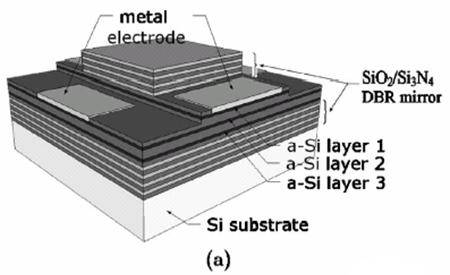
Fig. 1(a) Design schematic of the dual-wavelength amorphous Si detector. The high-reflectivity mirrors are comprised of alternating layers of SiO2 and Si-rich Si3N4. Three amorphous Si layers are sandwiched between the two mirrors and are separated by two SiO2 defect layers. Two pairs of metal electrodes connect the two amorphous Si layers. Each of the two photoconductive layers is sensitive to one single wavelength band.
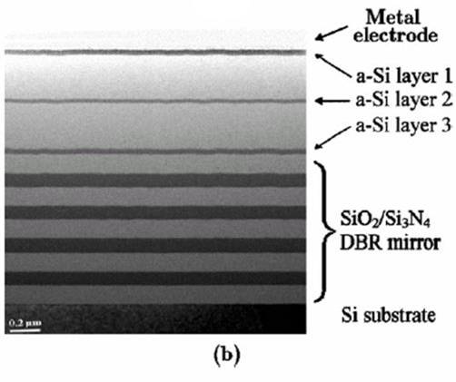
Fig. 1(b) High resolution cross-section TEM image of a photonic crystal pixel showing the uniform thickness and smooth interfaces of the photonic crystal stack.
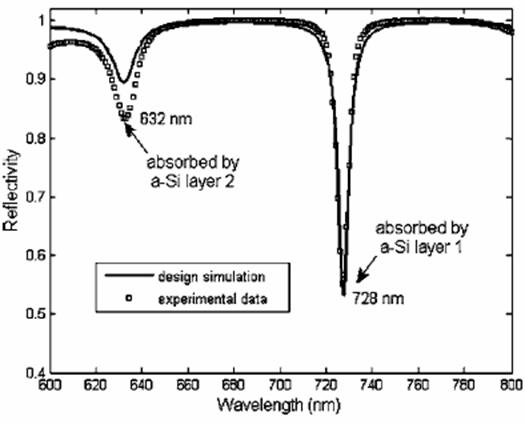
Fig. 2: Experimental data and transfer matrix simulation result of the photonic crystal stack reflectivity showing two resonant absorption peaks at 632 and 728 nm, which are selectively absorbed by the first two of the three amorphous Si layers.
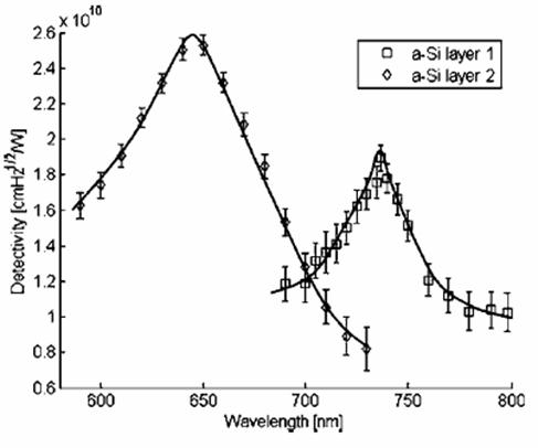
Fig. 3: Detectivity spectra at 10 V of the first two amorphous Si photoconductive layers showing wavelength selectivity. Detectivities are calculated from data measured using a tungsten halogen lamp monochromator. The measured resonance absorption peaks are significantly broadened due to two major effects. First, the various incidence angles of noncollimated light through an optical lens shift resonant peaks so as to increase the absorption peak bandwidth. The second effect is the fairly broad bandwidth of the incident light when the grating monochromator slit is tuned wider to enhance the incident optical flux.